Summary
South Korea is preparing to roll out three major projects designed to drive the next phase of national growth, anchored by a proposed semiconductor hub in the country’s southwest. The plan, which the presidential office has characterised as a national "great leap," will be unveiled around 0500 GMT and includes policy commitments from ministries covering industry, science, climate and transport.
Event and participants
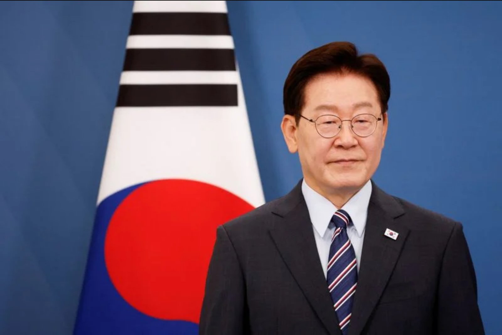
The announcement will be presided over by President Lee Jae Myung and is expected to feature investment proposals from major private-sector firms. Samsung Electronics and SK are reported by local media to be planning investment pledges, and the chairmen Jay Y. Lee and Chey Tae-won are among business leaders tipped to attend. The presidential office confirmed attendance by representatives of other companies including LG Electronics, HD Hyundai Robotics, Korea Electric Power Corp and Korea Water Resources Corp.
Scope of the package
Officials said the initiative will span three areas: semiconductors, AI data centres and physical AI such as robotics. The president’s social media posts indicated the establishment of a new chip cluster in the underdeveloped southwest, specifically naming Gwangju and South Jeolla province as focal areas. Local media reports have suggested the aggregated investments linked to the plans could exceed 1,000 trillion won ($651.41 billion) over coming years.
Policy and infrastructure support
The government will detail a broad set of support measures as part of the package. Those measures are expected to address electricity and water provision, land allocation, transportation and logistics infrastructure, workforce training and housing. Lee’s office said ministries responsible for industry, science, climate and transport will set out these policy supports at the unveiling.
President’s defence of the plan
President Lee has defended the proposed southwest chip hub in a series of posts on X, rejecting criticism that the initiative amounts to favouring a political stronghold. He framed the measure as a national strategy to correct regional imbalances and to expand semiconductor capacity for the AI era. In one post he wrote: "The creation of a semiconductor industrial ecosystem in (the southwest) is not a special favour for a particular region," and added, "It is the additional creation of the most rational semiconductor industrial centre through the decisions of relevant companies under full government support."
Industry considerations and constraints
Industry experts noted that diversifying chip investment beyond the Seoul metropolitan area could relieve existing infrastructure bottlenecks. At the same time, they cautioned that constructing advanced semiconductor fabrication plants requires vast quantities of electricity and water, sophisticated logistics, well-developed supplier networks and highly skilled labour - components that may not scale quickly enough in a newly developed region to meet rapidly rising AI-related demand.
Context and political response
Opposition politicians have sharply criticised the proposal, questioning whether the initiative is politically motivated given that 85% of voters in the southwest region backed Lee in last year’s presidential election. The unveiling arrives as Lee’s approval rating has declined for six straight weeks to 46.5%, according to pollster Realmeter.
Additional industry notes
South Korea is also home to SK Hynix, and the country hosts the world’s two largest memory chipmakers, whose high-bandwidth memory (HBM) chips are pivotal in the global race to build advanced AI systems. Both Samsung Electronics and SK Hynix already operate major semiconductor facilities in and around the Seoul metropolitan area.
Exchange rate note
At the time of reporting, $1 = 1,535.1300 won.