Covalent announced a collaboration with Oxford Instruments to broaden semiconductor characterization services by introducing wafer-level Raman and photoluminescence workflows. The combined capability is intended to enable non-destructive, spatially resolved analysis across whole wafers, addressing defect detection, stress and strain mapping, process development and failure analysis at full-wafer scale.
The partnership focuses on materials moving toward higher-volume manufacturing, specifically silicon carbide (SiC) and gallium nitride (GaN). These compound semiconductors demand inspection and analytics across entire wafers, a requirement that has been constrained in the past by limitations in throughput and scale.
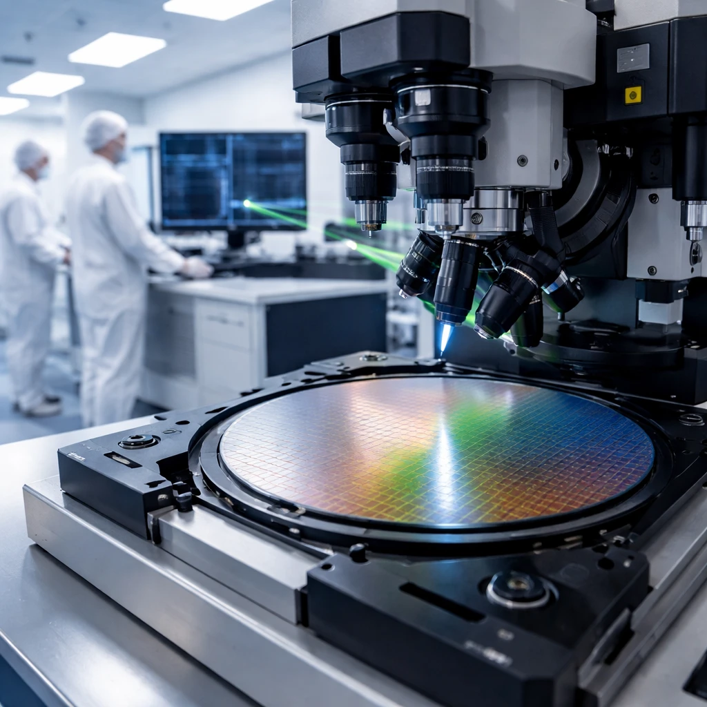
Technically, Covalent integrated Oxford Instruments’ WITec360TM Raman platform into its application environment and configured the system with dual laser excitation at 355 nm and 532 nm. That configuration supports surface-sensitive photoluminescence measurements together with high-resolution Raman imaging in a single unified workflow, tailored for compound semiconductor and advanced materials use cases.
The combined system can handle wafers up to 300 mm in diameter. Within a single integrated workflow, customers can perform wafer-level mapping of crystallinity, doping profiles, stress and defects, enabling characterization across the entire wafer rather than in localized regions.
Craig Hunter, CEO of Covalent, framed the announcement around practical outcomes for customers: "This is about expanding what our customers can do, not just what we can measure," he said. "We’ve taken Oxford Instruments’ powerful Raman technology and built it into workflows that directly support yield improvement, process control, and failure analysis at wafer scale."
Vahan Tchakerian, Senior Vice President of Sales & Applications at Oxford Instruments, emphasized the company’s Raman platforms and the role of the collaboration in production scaling. He said the instruments provide fast, high-resolution, non-destructive analysis of semiconductor materials on wafer sizes up to 300 mm and added, "By partnering with Covalent, we’re helping customers to bridge the gap from R&D to high-volume production, accelerating both development and manufacturing outcomes."
Implications
The integrated Raman and photoluminescence workflows position both firms to offer characterization that aligns with the needs of process engineers and failure analysis teams working on SiC and GaN wafers. By delivering wafer-level, spatially resolved analytics in a single workflow, the collaboration aims to reduce the barriers that previously limited full-wafer inspection in advanced materials production.