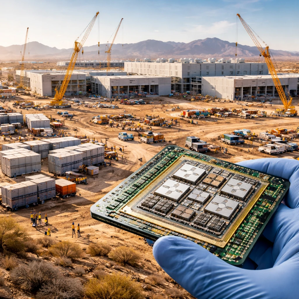
Santa Clara, California, April 22 - Taiwan Semiconductor Manufacturing Co is moving forward with plans to open an advanced chip packaging line in Arizona and targets bringing that capability into operation by 2029, company executives said.
Modern artificial intelligence chips are often assembled from multiple dies rather than a single monolithic piece of silicon. That assembly process relies on advanced packaging technologies - such as TSMC's CoWoS and 3D-IC - and has emerged as a supply constraint for companies that rely on these complex packages.
Earlier this year, TSMC indicated it had applied for permits to begin construction of its first advanced packaging plant in an existing Arizona facility but did not provide a timetable for when the new capability would be operational. At a conference in Santa Clara, executives updated that timeline and said physical work has already begun on-site.
"We are aggressively expanding our own capability within the Arizona facility," Kevin Zhang, deputy co-chief operations officer and senior vice president, said ahead of the conference. He added, "We are going to build a CoWoS capability and 3D-IC capability there before 2029, so that’s still our goal." The company framed those technologies as high-demand elements of its packaging portfolio.
Some major customers already source wafers from TSMC's Arizona factory, but a number of those chips continue to be shipped back to Taiwan for advanced packaging. The separation between front-end wafer fabrication in Arizona and back-end packaging in Taiwan has contributed to logistical complexity for multi-die AI packages.
In related developments, Amkor Technology previously said it was working with Apple and Nvidia on plans to build a packaging factory in Arizona with a target to be in place by mid-2027 and begin production by early 2028, a schedule that would be earlier than TSMC's stated 2029 goal. In 2024, Amkor and TSMC announced they would collaborate to bring several of TSMC's advanced packaging technologies to Arizona, although they have not released technical or commercial specifics.
Zhang described ongoing technology discussions between Amkor and TSMC as active. "We are partnering with them to see what kind of technology capability they can offer to our customers in order to accelerate some of the products to be manufactured in the U.S.," he said. "There are still some moving parts. I would say we are definitely looking at all possibilities to have a very diverse manufacturing footprint."
The company's statements indicate a concerted effort to expand domestic packaging capacity in the United States for advanced semiconductor assemblies, while leaving timing and some partnership details subject to further development.
Summary
TSMC has started construction to add CoWoS and 3D-IC advanced packaging capabilities at its Arizona facility and aims to have those capabilities operational before 2029. The expansion is intended to help alleviate packaging bottlenecks affecting AI chip production, and TSMC continues to explore partnerships and options to diversify manufacturing footprints in the U.S.
Key points
- TSMC plans to build CoWoS and 3D-IC packaging capabilities in Arizona and targets completion before 2029, with construction reported to have begun.
- Advanced packaging is a critical step for modern AI chips that combine multiple dies into single packages; current bottlenecks affect companies using these processes.
- Partnership discussions with Amkor are ongoing; Amkor has its own Arizona packaging timeline that would start production earlier than TSMC's stated target.
Risks and uncertainties
- Timing risk - TSMC's goal to have CoWoS and 3D-IC capabilities operational before 2029 remains a target and may be affected by construction or permitting developments; this impacts semiconductor manufacturing timelines.
- Partnership uncertainty - Discussions with Amkor and other partners are described as ongoing with "moving parts," leaving the exact technology contributions and operational arrangements unresolved; this affects supply-chain coordination in packaging and assembly.
- Logistics and capacity constraints - Until advanced packaging is established domestically in Arizona, some wafers from the U.S. facility continue to be sent back to Taiwan for packaging, maintaining cross-border logistical complexity for AI chip production.