Overview
Bernstein has pointed to specific vendors that supply the tools and materials underpinning advanced semiconductor packaging and test flows, noting that growing AI chip demand and more complex stacking approaches are making these capabilities increasingly central to chipmakers. The firms highlighted provide grinding, dicing, bonding and testing equipment or related substrate and interconnect materials used across advanced packaging processes.
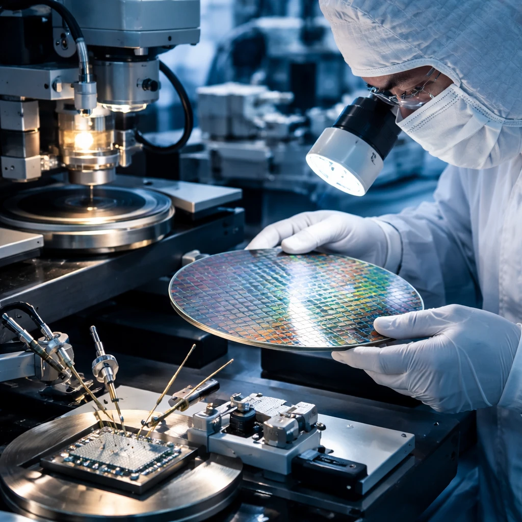
Why advanced packaging matters
The research note argues that as chipmakers move to sophisticated stacking methods and advanced package architectures to meet the performance and density requirements of AI workloads, equipment and material specifications for those processes will become more demanding. That evolution is expected to raise the importance of suppliers that enable wafer preparation, precise die separation, robust bonding solutions and thorough final testing.
Bernstein’s top company selections
Bernstein identified four companies it views as positioned to benefit from this shift. Each is singled out for specific capabilities or market positions that map to advanced packaging needs.
-
DISCO - Bernstein highlights DISCO as the dominant supplier in grinders and dicers, equipment it says is required across many stacking and advanced packaging processes. The firm expects an acceleration in CoWoS capacity growth and anticipates that HBM capital expenditure will resume growth alongside continued AI momentum. Bernstein also foresees acceleration in wafer-to-wafer bonding with NAND stacking adoption at Kioxia and potentially Samsung, together with the adoption of BSPDN at TSMC. As stacking technologies progress, Bernstein expects grinder and dicer specifications to tighten, which it projects would lift average selling prices and deepen DISCO’s competitive moat. On results, DISCO reported a 9.7% increase in group operating profit for the first nine months of its fiscal year, and its preliminary third-quarter orders and sales exceeded company expectations.
-
Advantest - The research note positions Advantest to benefit from strong system-on-chip testing demand as testing time grows with chip complexity. Bernstein highlights the potential for greater test insertions, including expanded wafer-level and die-level testing. The firm also notes that migrations in high-bandwidth memory - from HBM to HBM4 and later to HBM4E - could drive higher testing intensity. In a recent update, Advantest announced third-quarter results that beat analyst forecasts, reporting revenue of 273.8 billion yen and earnings per share of 108.41 yen.
-
BE Semiconductor - Bernstein views BE Semiconductor as a long-term winner in the advanced packaging era, citing its pioneer status and near-monopoly market share in die-to-wafer (D2W) hybrid bonding. The note acknowledges that the timing of hybrid bonding adoption may not be immediate but indicates the firm believes adoption in logic chips and HBM is likely over time. BE Semiconductor reported a 43% sequential increase in preliminary fourth-quarter orders, which Bernstein attributes to demand for data center applications. The research piece also notes that, separately, Bernstein SocGen Group lowered its price target on the company, citing slower adoption of certain bonding technology.
-
Ibiden - Bernstein highlights Ibiden’s gains from ABF substrate upgrades and the adoption of new technologies such as Embedded Multi-die Interconnect Bridge. The note observes that Nvidia’s Rubin substrate migration is approaching and that ABF content value is expected to double. Bernstein suggests Ibiden is likely to regain share from Unimicron in Rubin-related products and to retain a dominant market position supplying Nvidia substrates.
Takeaways
Bernstein’s coverage foregrounds a set of specialized suppliers across grinding, dicing, bonding and testing who are tied directly to the technical steps required for advanced packaging and chip stacking. The research frames these companies as strategically important to chipmakers pursuing higher performance, particularly for AI-oriented workloads that push packaging and interconnect complexity.
Limitations and scope
The note presents expectations for capacity growth and technology adoption, and it reports recent corporate results and preliminary orders cited by the companies. It does not provide a detailed timeline for adoption of the various bonding and packaging technologies, and it notes differences in timing and adoption across suppliers and end markets.
Editor’s note
This article summarizes views attributed to Bernstein as described above and reports the company-specific results and preliminary order information referenced in that coverage.