Senior figures from China’s chip industry have proposed a concentrated national effort to assemble fully operational lithography systems within the 2026-2030 window, underscoring Beijing’s drive for greater technological self-reliance.
The appeal was set out in a joint article published online late Wednesday by Zhao Jinrong, chairman of Naura Technology Group; Chen Nanxiang, chairman and president of Yangtze Memory Technologies Corp; and Liu Weiping, chairman of Empyrean Technology, together with leading semiconductor institutes. In that piece they urged the central government to pool national resources so that technological advances achieved across multiple institutions can be integrated into complete systems.
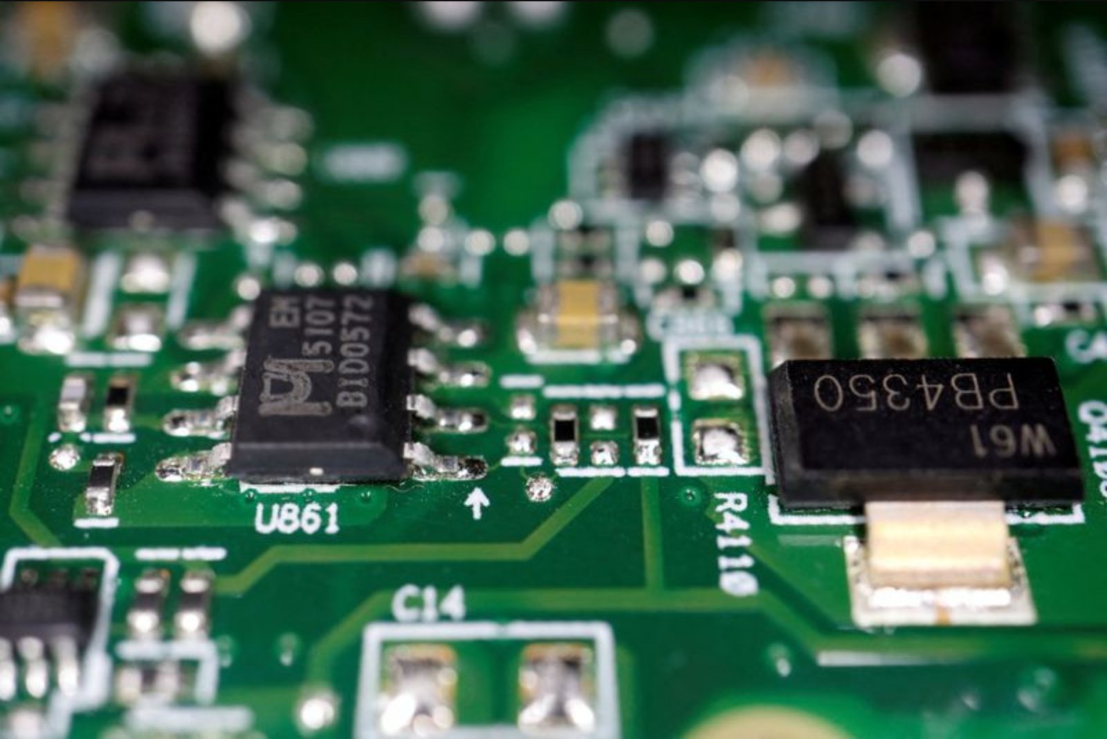
The executives placed lithography machines at the center of their argument, noting the complexity of existing market leaders’ equipment. "Taking lithography machines as an example, ASML’s extreme ultraviolet (EUV) equipment has 100,000 components supplied by 5,000 suppliers, with ASML merely serving as the integrator," they wrote in Science and Technology Review, a journal affiliated with China’s science and technology professionals association. They argued that building a domestic integration capability is urgent and requires unified allocation of funds and human capital.
"How to establish China’s ASML, so that the ’integrated’ can jump out of the barrier of ’fame and fortune’, and uniformly allocate funds and human resources is an urgent issue that relevant departments should immediately formulate implementation plans," the authors added.
The call for a national program comes amid an intensifying technology competition with the United States. Since 2020 Washington has applied restrictions aimed at preventing China from expanding advanced production capacity below the 7-nanometer node. The article referenced this strategic context while laying out the technical hurdles that remain.
On the technical front, the authors said Chinese institutions have made breakthrough progress in several critical subsystems for EUV lithography, including EUV laser light sources, wafer stages, and optical systems. Despite those advances, they emphasized that the challenge of integrating these subsystems into a complete, operational lithography machine persists and must be addressed within the 15th five-year plan period.
Beyond mechanical and optical integration, the article identified additional bottlenecks that require coordinated national attention. These include electronic design automation (EDA) software and materials such as silicon wafers and specialty electronic gases. The authors argued that resolving these bottlenecks would demand centralized planning and resource allocation.
In the government’s latest work report released on Thursday, semiconductors were named as a core pillar of nascent industries alongside aviation, biotechnology and the low-altitude economy. The report highlighted domestically driven breakthroughs in chip research and development, a point the executives noted. However, the five-year roadmap did not explicitly single out lithography machines; it instead called to "improve advanced process manufacturing capabilities, accelerate the development of key equipment, materials and components."
The joint article also cited China’s current standing in more mature technology nodes. It noted that China’s chip production capacity at the mature 28nm node and above accounts for 33% of global capacity and remains unrestricted in both manufacturing and design, according to the Science and Technology Review piece.
As part of their recommendations, the executives proposed establishing public platforms equipped with the most advanced process capabilities. These platforms would be tasked with researching, developing and verifying the latest device structures, process equipment, components, materials and EDA software. The intent would be to provide centralized facilities where integration and validation of new technologies could take place under unified oversight.
Key points
- Senior Chinese semiconductor executives urged a coordinated national push to deliver operational lithography systems during 2026-2030, calling for pooled funding and personnel to achieve integration.
- While individual subsystems such as EUV laser sources, wafer stages and optical elements have seen breakthrough progress, integrating these into full machines remains a major technical challenge.
- The article highlighted bottlenecks in EDA software and materials like silicon wafers and electronic gases, and recommended public platforms with advanced process capabilities to test and verify innovations.
Risks and uncertainties
- Integration risk: Despite subsystem breakthroughs, converting component-level advances into a complete working lithography system is unresolved and could delay domestic capability - this affects equipment manufacturers and semiconductor fabs.
- Supply-chain bottlenecks: Limitations in EDA tools and critical materials such as wafers and specialty gases are identified constraints that could impede scale-up - these risks touch materials suppliers and chipmakers.
- External restrictions: Export controls aimed at restricting China’s expansion below the 7-nanometer node remain a factor influencing access to technologies and components, which can impact investment and production planning in advanced semiconductor segments.